- Apple’s chiplet era has started. M5 Pro is Apple’s first Pro chip with two main dies. But it can still work like one chip and support unified memory.
- M5 Pro is better for local AI development. With up to 64GB unified memory and high memory bandwidth, it can run local AI models more smoothly.
- Counterpoint's in-chip teardowns can reveal Apple's true chip design direction. It provides an analysis of chip layout, key modules, memory design, and packaging details.
- AI computing is now more important in the GPU. Each GPU core has a Neural Accelerator. This helps M5 Pro offer much stronger AI performance than M4 Pro.

Apple M5 Pro is Apple’s first Pro-series dual-die chip and marks the start of the brand’s chiplet era. On the surface, the specs look similar to past generations, with an 18-core CPU, up to 20-core GPU, and LPDDR5X-9600 unified memory. But inside, the M5 Pro has a very different design compared to previous Apple Silicon chips.
Counterpoint Research has conducted a complete teardown of the latest MacBook Pro A3426, covering the device structure, PCB design, heat dissipation system, the M5 Pro chip itself, its packaging, and in-chip teardown analysis. This helps us identify Apple’s semiconductor design approaches and improvements in the AI PC era, showcasing significant system integration capabilities. This also highlights design and architectural improvements in high-performance computing, AI inference, and advanced packaging technology approaches.
In this report, we break down the M5 Pro and emphasize three pivotal architectural changes that aim to shape Apple Silicon for the AI era.
Three Shifts in One Generation
- Apple's chiplet era begins. The M5 Pro chip uses four separate dies, including one CPU die, one GPU die, and two dummy dies, connected by TSMC's advanced packaging SoIC-MH translating into Apple’s new flexible Fusion Architecture bringing in greater bonding density, resulting in faster and shorter connections thus higher speeds and lower power consumption. Apple also maintains Unified Memory across both dies, so the system operates as a single chip. This is the key difference compared to AMD and Intel chiplet designs.
- AI computing moves into the GPU. For the first time, each GPU core includes a Neural Accelerator, while the SoC also features a separate 16-core Neural Engine. This greatly improves AI performance, with GPU AI throughput reaching 4 times higher than M4 Pro. However, how Apple is thinking about AI workload orchestrator to help developers dynamically push specific workloads to respective neural accelerators in GPU or NPU for more efficient heterogeneous computing.
- Highest memory bandwidth ever in an Apple Pro-tier SoC. M5 Pro uses LPDDR5X-9600 memory with 307 GB/s bandwidth and up to 64 GB unified memory. This gives M5 Pro enough memory capacity and bandwidth to support larger local LLM inference and professional on-device AI workflows.
Inside the CPU Die

The M5 Pro features an 18-core CPU, including six Super Cores and 12 Performance Cores based on Armv9 instruction set. Apple also integrates a 16-core Neural Engine and four Thunderbolt 5 controllers into the chips. The Super Cores may run at a higher frequency than the Performance Cores. Also, the M5 Pro CPU die includes other potential blocks, such as the SSD controller and System Level Cache.
Apple uses the same CPU die for both M5 Pro and M5 Max. The main difference between the two chips is the GPU die, showing Apple’s clear chiplet and binning strategy.
Inside the GPU Die
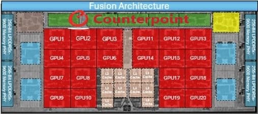
The GPU die contains the 20-core GPU complex for the top SKU configuration. Each GPU core now includes a Neural Accelerator that supports FP16 and INT8 matrix operations. This new architectural design is the main reason for the 4x improvement in AI computing performance. Around the edge of the die, there are four LPDDR5X-9600 memory controllers and PHYs, four Display Engines that can support one internal and three external displays, and a Media Engine with the Video Encoder, Decoder, AV1 Decoder, and ProRes Engine. The ProRes Engine is also the largest single block inside the Media Engine complex.
Process Technology: TSMC N3P Under FIB
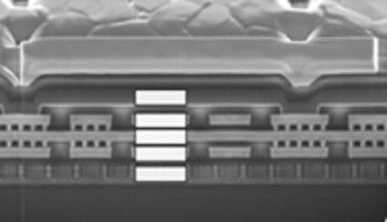
Both dies in M5 Pro are made with TSMC’s N3P process. N3P is the third generation of TSMC’s 3nm technology family. It is an optical shrink of N3E, while still keeping full design-rule and IP compatibility. According to TSMC, N3P can deliver about 5% higher performance at the same leakage level, 5% to 10% lower power at the same frequency, and around 4% higher transistor density for mixed designs, including 50% logic, 30% SRAM, and 20% analog. Though, it remains to be seen how Apple’s new architectural and design choices can help touch these physical performance ceilings.
One important point is that N3P still uses FinFET transistors. Gate-all-Around, or GAA nanosheet technology, only starts with TSMC N2, which entered volume production in Q4 2025. This means M5 Pro could be one of the last major consumer Apple Silicon generations based on FinFET. Future M-series chips using N2 are expected to move to nanosheet transistor structures.
TSMC N3P Process Technology – Key Parameters

Advanced Packaging: SoIC-mH Implementation
The two dies are connected by Apple’s Fusion Architecture, which Apple describes as an advanced packaging design that connects two third-generation 3nm dies into a single SoC. Market reports and teardown analysis indicate that this implementation is likely based on TSMC SoIC-mH. SoIC refers to System on Integrated Chips, while “mH” is commonly reported as “molding horizontal.” This is one type of TSMC’s hybrid bonding technology, designed for high-density chiplet integration. Apple’s M5 Pro/Max is one of the first high-volume consumer-class SoC designs publicly described by Apple as using a two-die advanced packaging architecture.
For Apple, the new horizontal architecture offers several important benefits. It allows the CPU and GPU dies to be separated horizontally across a larger molded area. It also helps spread thermal hotspots. This is very important for laptops, because their sustained power is usually around 30-40 W. At the same time, it maintains the high-bandwidth, low-latency die-to-die communication required for Apple’s Unified Memory Architecture.
Additionally, it can provide very low die-to-die latency. This allows the software to treat the two dies almost like one complete chip.
As a result, Apple can keep its Unified Memory Architecture working smoothly across the die boundary. This is very important because the software does not need to manage the two dies separately. This makes Apple’s Fusion Architecture different from many traditional chiplet designs, where the die boundary may have a bigger impact on the system architecture.
Why M5 Pro Matters
For developers and end users, the M5 Pro makes the MacBook Pro one of the most ideal local AI development platforms. This is especially important for 7 billion to 13 billion-parameter models, because the combination of up to 64 GB unified memory and 4× higher GPU AI performance can become a key advantage.
For the chip industry, the M5 Pro also shows that Apple’s ambition is no longer only about leading in performance per watt. Apple is also moving into advanced packaging and memory innovation, areas that were mainly handled by data center accelerator vendors before 2026.
According to our Foundry Tracker & Forecast, the M5 series will likely account for 18.4% of total PC CPU wafer consumption in 2026, up significantly from 4.2% a year ago.
The chiplet era of Apple Silicon has begun.
What the Full Report Will Cover
Our full M5 Pro in-chip teardown analysis will include several detailed parts:
- Full floor-plan extraction of both dies using optical microscopy, including IP block identification, block-level size measurement, and layout comparison between the CPU die and the GPU die.
- SoIC-mH packaging characterization.
- Unified memory architecture characterization, including the number of LPDDR5X memory stacks, memory interface width, bandwidth calculation, memory placement inside the package.
- Process node verification and parameter extraction through FIB cross-section analysis, including transistor geometry, contact/gate pitch, M-layer thickness, BEOL metal stack structure, die size, and other key physical measurements used to evaluate the underlying process technology.
If you are interested in subscribing to the full report or would like to learn more, please contact us at [email protected].


