
OFC에서 확인된 핵심 메시지는, 이제 네트워킹이 단순한 연결을 넘어 컴퓨팅 인프라의 핵심 구성 요소로 자리잡았다는 점이다. 엔비디아(NVIDIA)가 행사 기간 중 공개한 약 20억 달러 규모의 루멘텀(Lumentum) 및 코히런트(Coherent) 투자 역시, 세계 최대 반도체 기업이 광(옵틱스)을 GPU 로드맵의 핵심 요소로 보고 있음을 보여준다. 이에 따라 AI 칩과 광 부품 간 통신이 이번 행사에서 주요 화두로 부각됐으며, 새로운 개방형 표준 기반 멀티벤더(MSA) 커넥터 발표가 이를 더욱 강조했다.
오픈 표준 MSA(Multi-Source Agreements)
이번 행사에서는 두 가지 새로운 오픈 표준 커넥터 협약이 발표됐다. 여기에 2주 전 발표된 XPO MSA까지 포함하면, 현재 AI 시대의 전력·대역폭 문제 해결을 목표로 하는 서로 다른 3개의 커넥터 표준이 경쟁 구도를 형성하게 된다. 이들 표준은 모두 특정 벤더에 종속된 구조에서 벗어나려는 공통된 방향성을 가지며, 각각 데이터센터 아키텍처의 다른 영역을 타깃으로 한다.
- 고집적 플러그형 광학 (XPO)
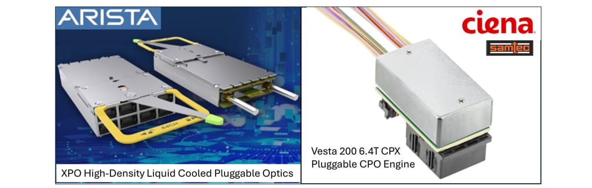
아리스타 네트웍스(Arista Networks)가 주도하는 XPO MSA는 차세대 플러그형 광 트랜시버 폼팩터로, 액체 냉각 기능까지 통합된 것이 특징이다. 핵심 목표는 서버 랙 전면(faceplate) 공간 내에서 최대한 많은 대역폭을 집적하는 것이다. 주요 창립 멤버로는 코히런트, 라이트매터(Lightmatter), 마벨(Marvell), 마이크로소프트(Microsoft), 테라홉(TeraHop), 그리고 커넥터 기업인 몰렉스(Molex)와 삼텍(Samtec) 등이 참여하고 있다. - 오픈 코패키징 표준 (Open CPX MSA)
Open CPX MSA는 NPO(Near-Package Optics)와 CPO(Co-Packaged Optics) 영역을 겨냥한 표준으로, 서버 내부 ASIC 바로 옆에 장착 가능한 플러그형 소켓 표준을 정의한다. 창립 멤버에는 시에나(Ciena), 마벨, 코히런트, 마이크로소프트, 테라홉, 그리고 몰렉스, 삼텍 등이 포함된다. - OCI MSA (Optical Compute Interconnect)
엔비디아, AMD, 메타(Meta), 브로드컴(Broadcom), 오픈AI(OpenAI) 등이 주도하는 OCI는 물리 및 전기 계층을 정의하는 표준이다. 여기에는 SerDes 인터페이스, 패키징, 핀 구성, 그리고 WDM(파장 분할 다중화) 기술이 포함된다. 목표는 광 엔진, 레이저 등 다양한 광 부품을 포함하는 플러그 앤 플레이 방식의 OCI 생태계 구축이다. 다만 논리 계층은 포함되지 않는다.
아리스타의 XPO와 시에나/샘텍의 CPO 기반 플러그형 광학 솔루션
참가기업
전시장은 800G 및 1.6T 네트워킹, 다양한 CPO·NPO·LPO·XPO 데모, 통합 레이저 제품, 중공(core) 광섬유 도입 계획 등 차세대 AI 팩토리를 겨냥한 기술들로 채워졌다. 주요 기업들의 핵심 발표 내용은 다음과 같다.
Ayar Labs
아야랩스(Ayar Labs)는 자사의 핵심 기술인 TeraPHY 광 I/O 칩렛과 수퍼노바(SuperNova) 원격 레이저의 최신 진화를 공개했다. TeraPHY I/O 칩렛은 양방향 기준 8Tb/s(각 방향 4Tb/s)의 대역폭을 구현하며, UCIe 표준을 기반으로 NV링크(NVLink), CXL, 이더넷(Ethernet) 등 다양한 프로토콜을 유연하게 지원한다. 수퍼노바 레이저는 액체 냉각 기반 외장형 광원(ELSFP) 구조로 설계됐다. GPU와 레이저를 분리하고 액체 냉각을 적용함으로써 광 링크의 신뢰성과 수명을 높이는 것이 특징이다.
또한 아야랩스는 ODM 파트너 Wiwy nn(Wiwynn)과 협력한 CPO 기반 랙스케일 시스템도 공개했다. 양사는 최대 1,024개의 AI 가속기를 하나의 통합 시스템으로 연결하는 광 기반 랙스케일 레퍼런스 디자인을 개발 중이다. UALink 표준 기반으로, 해당 시스템은 아야랩스의 TeraPHY 광 엔진과 수퍼노바 레이저를 Wiwynn의 차세대 800V HVDC 랙 설계에 통합하는 구조다. 하이퍼스케일 및 클라우드 고객 대상 상용화는 2026년 말~2027년 사이 시작될 것으로 예상된다.
Ciena
OFC에서 시에나는 AI 인프라 중심으로 전략을 전환하며, 대규모 데이터센터 인터커넥트(DCI)와 GPU 클러스터 내부를 연결하는 네트워크 패브릭 공급업체로 포지셔닝했다.
시에나는 WaveLogic 6 Extreme(WL6e) 코히런트 기술의 상용 준비 상태를 공개했으며, 단일 파장에서 1.6Tb/s를 지원하는 업계 최초 수준의 성능을 구현했다. 또한 기존 장거리 네트워크 중심 전략에서 벗어나, 최근 인수한 누비스 커뮤니케이션즈(Nubis Communications) 기술 기반으로 데이터센터 내부용(intra-DC) 제품 2종을 공개했다.
- Vesta 200 6.4T Optical Engine
: 업계 최초 개방형 생태계 기반 플러그형 CPO 솔루션 스위치 칩 바로 옆에 광 모듈을 배치해 AI 클러스터 전력 소모 절감 목적 - Nitro 2004 Copper Cable Extender
: DAC(고속 구리 케이블) 전송 거리를 확장하는 리니어 드라이버 AEC 대비 최대 80% 전력 절감 가능
두 제품 모두 2026년 2분기 고객 샘플링이 예정되어 있다.
Lightmatter
보스턴 기반 라이트매터는 Passage L20 광 엔진, L-Series CPO 솔루션, vClick 분리형 광 커넥터, Guide VLSP 광 엔진, Passage EVK50 평가 키트 등 다양한 데모를 공개했다.
- Passage L20
3D 적층 기반 6.4Tb/s 광 엔진으로, NPO 및 OBO(보드 단 광) 애플리케이션을 겨냥한 솔루션이다. 기존 플러그형 트랜시버와 코패키징(CPO) 사이의 중간 단계 기술로 볼 수 있으며, BiDi(양방향) 다중화를 적용해 필요한 광섬유 수를 절반으로 줄였다. - L20은 업계 표준 224G PAM4 전기 인터페이스를 사용하는 ‘드롭인(drop-in)’ 칩으로, 전체 칩 아키텍처를 재설계하지 않고도 쉽게 적용할 수 있다. 라이트매터는 고성능 스위치에서 L20 16개로 기존 플러그형 모듈 512개를 대체할 수 있다고 밝혔다. 고객 대상 샘플링은 2026년 말 시작될 예정이다.
- Passage L-Series
L200과 L200X 칩렛으로 구성된 이 시리즈는 10만 개 이상의 GPU가 필요한 초대형 AI 학습 클러스터를 겨냥한 보다 급진적인 아키텍처다. L20이 칩 가장자리에서 통신하는 방식이라면, L-Series는 3D 적층 구조를 통해 칩 전체 표면에서 광 연결이 가능하도록 설계됐다. 이를 통해 16파장 DWDM 기반으로 광섬유 한 가닥당 최대 1.6Tb/s 속도를 구현할 수 있다. 이 칩렛은 UCIe 표준을 기반으로 하며, 퀄컴(Qualcomm)과 공동 개발됐다. 2026년 말 샘플링이 예정돼 있다. - vClick FAU
라이트매터는 vClick 분리형 광 파이버 어레이 유닛(FAU)도 공개했다. 이 기술은 고성능 AI 칩을 위한 플러그형 광 인터페이스를 구현해, 기존의 광 연결 방식을 보다 간편하게 사용할 수 있도록 한다. - Guide VLSP Light Engine
8~16개의 파장을 사용하는 DWDM 레이저 엔진으로, 높은 파장 정확도와 동적 파장 튜닝을 통한 자체 복구 기능을 갖춘 것이 특징이다.
Nokia
노키아(Nokia)는 인피네라(Infinera) 인수(23억 달러) 이후 OFC26에서 AI 네이티브 네트워킹 중심으로 전략을 전환했다. 핵심은 단일 하드웨어 구조에서 벗어나 모듈형 빌딩블록 방식으로 전환하고, 이를 통해 총소유비용(TCO)을 낮추는 것이다.
- Four Engines DSP 전략
단일 플래그십 칩 대신 온타리오, 휴론, 슈페리어, 퍼시픽 등 네 가지 DSP를 도입해 다양한 광 인터페이스와 조합할 수 있도록 했다. 이를 통해 총 13개 이상의 애플리케이션 맞춤형 제품 구성이 가능하다. 온타리오와 휴론은 1.6Tb/s 이하의 저전력 플러그형 중심으로 데이터센터 및 메트로 환경에 적합하며, 슈페리어는 2.4Tb/s급 엔진으로 표준 플러그형의 전력 제약을 넘어 최대 광 용량을 구현하는 데 초점을 맞췄다. - 1.6T 및 3.2T 코히런트 솔루션
Nokia는 2027년 중반 샘플링을 목표로 1.6T 플러그형과 3.2T 저전력 코히런트 솔루션을 포함한 새로운 제품군을 공개했다. 이 솔루션은 특히 캠퍼스 및 엔터프라이즈 환경의 단거리 AI 클러스터에 최적화되어 있다. - 업계 최초 양면 플러그형 기술
스케일아웃 네트워크를 위해 설계된 기술로, 서로 다른 고속 네트워크 구조 간 연결을 단순화하는 것이 목적이다. 예를 들어, LPO나 CPO 스위치의 출력을 별도의 장비 없이 바로 장거리 코히런트 신호로 변환할 수 있어 추가 케이블이나 트랜스폰더가 필요 없다. Nokia는 2nm 및 3nm DSP와 결합할 경우, 이 기술을 통해 하이퍼스케일 데이터센터에서 총소유비용을 최대 70%까지 절감할 수 있다고 밝혔다.
OpenLight Photonics
오픈라이트포토닉스(OpenLight Photonics) 는 PASIC(광 애플리케이션 특화 집적회로) 설계 및 제조에 집중하는 기업으로, 타워세미컨덕터를 통해 PDK(Process Design Kit)와 레이저, 변조기, 증폭기 등 다양한 구성 요소 라이브러리를 제공한다. 이를 통해 다른 기업들도 오픈라이트의 IP를 활용해 자체 맞춤형 광 칩을 설계할 수 있다.
기존 실리콘 포토닉스 산업에서는 레이저를 실리콘 칩에 직접 통합하는 것이 가장 큰 기술적 난제 중 하나였다. 오픈라이트는 이 문제를 이종 집적(heterogeneous integration) 방식으로 해결했다. 이는 인듐인화물(InP) 소재를 실리콘 웨이퍼 위에 직접 접합하는 공정을 의미한다. OFC에서 OpenLight는 다음과 같은 내용을 발표했다.
- Electro-Absorption Modulator (EAM)
오픈라이트는 400G/lane급 EAM을 공개했으며, 이는 3.2Tb/s 광 트랜시버 구현의 핵심 기술이다. 또한 3.2T DR8 구조의 포토닉 집적회로(PIC) 초기 프로토타입을 이미 여러 트랜시버 업체에 샘플 공급했다고 밝혔다. - 완전 통합형 1.6T DR8 평가 보드
레이저, 변조기, 증폭기, 포토디텍터를 하나의 플랫폼에 모두 통합한 고속 광 링크 시스템을 시연했다. 이 시스템은 마벨(Marvell)의 3nm 기반 Ara 1.6T DSP와 연동해 동작하는 모습이 공개됐다.
또한 상업화 측면에서도 중요한 진전을 이뤘다. 오픈라잇는 800G 및 1.6T 레이저 통합형 PIC에 대해 대량 생산 주문을 확보했다고 밝혔다.주요 고객으로는 뉴 포토닉스(New Photonics)가 언급됐으며, 해당 기업은 오픈라이트 플랫폼을 기반으로 양산 체제에 진입하고 있다.
Scintil Photonics
프랑스 그르노블에 기반을 둔 신틸 포토닉스(Scintil Photonics)는 CEA-Leti에서 분사한 스타트업이다. 오픈라이트와 마찬가지로, 실리콘 포토닉스의 핵심 과제인 ‘레이저의 칩 내 직접 통합’을 해결하는 데 집중하고 있다. 두 회사 모두 인듐인화물(InP) 레이저를 실리콘 웨이퍼에 직접 접합하는 방식으로 접근하고 있다.
신틸은 팹리스 형태로 자체 광 엔진과 완전 통합형 회로(예: LEAF Light)를 개발하는 기업이며, 특히 DWDM(고밀도 파장 분할 다중화) 레이저 기술 상용화에 집중하고 있다. 최근에는 대량 생산 단계로 전환하고 있다고 밝혔다. OFC 2026 주요 발표 내용은 다음과 같다.
- LEAF Light 평가 키트(EVK)
CPO 기반 AI 스케일업 네트워크를 위해 설계된 업계 최초 단일 칩 DWDM 레이저 소스 플랫폼을 공개했다. 이 키트를 통해 칩셋 업체들은 Scintil의 다중 파장 통합 기술이 차세대 프로세서와 어떻게 동작하는지 검증할 수 있다. - 타워 세미컨덕터 협력
신틸과 타워 세미컨덕터는 SHIP(Scintil Heterogeneous Integrated Photonics) 기술의 성과를 공개하고, 해당 공정이 타워 세미컨덕터의 대량 생산용 실리콘 포토닉스 플랫폼에서 이미 양산 가능한 수준에 도달했다고 밝혔다. 이는 인듐인화물 레이저를 실리콘 웨이퍼에 직접 접합하는 복잡한 공정이 월 수십만 개 규모로 생산 가능하다는 것을 의미하는 중요한 이정표다.
수출 바우처 상담 문의
(카운터포인트 Email: [email protected], 02-553-4813)
카운터포인트리서치는 기술 생태계 전반에 걸쳐 시장 데이터, 인사이트, 리포트 및 컨설팅 서비스를 제공하는 글로벌 산업 및 시장 조사 기관입니다. 반도체 제조사, 부품 공급업체, 소프트웨어 및 애플리케이션 개발자부터 통신 서비스 제공업체, 유통 채널, 투자자에 이르기까지 공급망 전반에 걸친 다양한 글로벌 고객에게 자문을 제공합니다.
[카운터포인트리서치]
경험이 풍부한 당사의 애널리스트 팀은 전 세계 주요 혁신 허브, 제조 클러스터, 주요 상업 중심지에 위치한 글로벌 오피스를 통해 고객을 지원하고 있습니다. 기업 내 최고경영진(C-suite)부터 전략, 시장 인텔리전스, 공급망, 연구개발(R&D), 제품 관리, 마케팅, 영업 등 다양한 부서와 지속적으로 소통하고 있습니다.
카운터포인트 주요 연구 분야
: 인공지능(AI), 자동차, 클라우드, 커넥티비티, 소비자 가전, 디스플레이, eSIM, IoT(사물인터넷), 위치 기반 플랫폼, 거시경제, 제조, 네트워크 및 인프라, 반도체, 스마트폰 및 웨어러블 기기 등 공개된 시장 데이터, 인사이트 및 리포트를 확인하고, 애널리스트와의 소통을 원하시면 카운터포인트 라이브러리를 방문해 주세요.


