The rapid advancements in AI have been driven primarily by an exponential growth in the size and complexity AI models. Over the past decade, AI models have evolved from relatively simple algorithms to complex Large Language Model (LLM) architectures with unprecedented capabilities. However, AI is no longer limited to LLMs and is being applied to many domains resulting in different types of workloads. As workloads diversify, so too must the infrastructure, i.e. “a one size fits all” type data center infrastructure will not suffice, as each workload will have its own specific requirements.
Key Benefits of Customization
Customizing an AI data center no longer involves just customizing the compute elements, i.e. the XPUs, but potentially includes all components in an AI server or rack. Key benefits of infrastructure customization include:
Performance Optimization - training LLMs or running inference at scale are highly specialized tasks. Custom silicon can be tuned for specific operations, such as matrix multiplications (used in neural networks), sparse computation, low-precision arithmetic (for example, FP8, INT4), etc.
Rapid Evolution of AI Models – AI model architectures are evolving rapidly. Custom silicon can be designed for specific algorithms, resulting in improved performance compared to general-purpose chips.
Improved Power and Thermal Efficiencies - data centers running massive AI workloads consume tremendous amounts of energy. Custom silicon designed for specific workloads will result in improved performance-per-watt efficiencies – up to 30% according to hyperscalers - which results in lower power consumption and reduced cooling requirements.
Reduced Total Cost of Ownership (ToC) – although custom silicon chips have high upfront costs, the improved power and thermal efficiencies plus higher performance/throughput results in reduced ToCs in the long-term, particularly in the case of major hyperscalers running massive AI workloads at scale.
Differentiation and Competitive Advantages – hyperscalers want to differentiate their AI services and develop their own, unique proprietary hardware/software stacks. Custom silicon can also include specialized security functions such as memory encryption designed specifically to meet customers’ requirements.
Custom Silicon Opportunities
Modern AI infrastructure requires complete platforms with silicon to run AI workloads at scale. In addition to custom XPUs, an AI accelerated compute platform requires a multitude of companion chips - known as XPU attach chips - to support and scale the XPUs. Examples include network interface cards (NICs), power management ICs, specialized coprocessors for security and host management, memory poolers/expanders, etc.
Within an XPU, there are multiple customization opportunities, including in the core architecture, the number of cores, the ratio of cores to memory and the level of precision required (FP16, FP8, FP4, etc.). Another key component ripe for customization is memory, which has for a long time rigidly followed standards. However AI, with its need for massive amounts of memory and bandwidth, is changing this. Marvell recently made two important announcements regarding customised HBM and SRAM chips for AI data centers.
Customized HBM
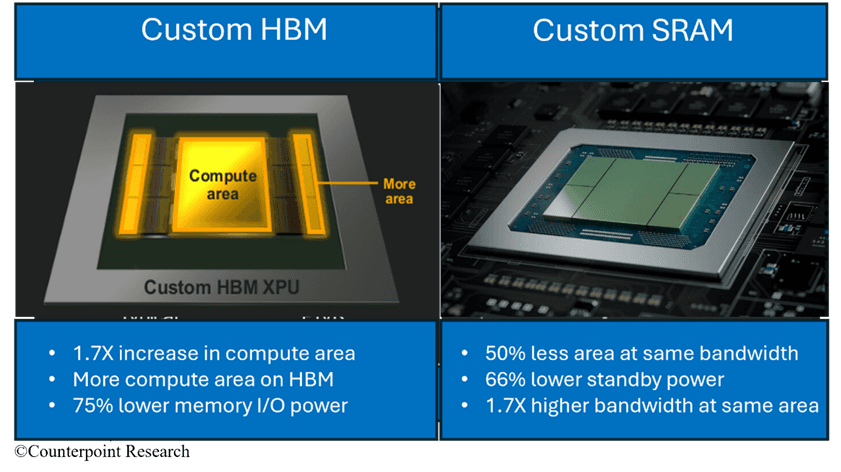
HBM is a critical component within an XPU and accounts for around 40% of the total cost. Current HBMs feature an I/O memory which uses JEDEC-based interfaces, typically consisting of 32 64-bit channels. However, Marvell has developed a custom HBM compute architecture which uses smaller, optimized interfaces (Figure 1, left). This reduces the silicon real estate in each die allowing the HBM support logic to be integrated onto the base die.
Marvell’s customized HBM solution results in higher XPU performance while providing 75% lower interface power consumption compared to standard JEDEC-based interfaces. Reducing HBM size also provides 25% more real estate. Customers can leverage these savings to add more compute or HBM memory per XPU – or add new features.
Customized SRAM
SRAM memory chips sourced from foundries or IP providers occupy an incredibly large area inside an XPU – typically up to 40%. In June, Marvell announced the industry’s first 2nm custom SRAM chip occupying 50% less area at the same bandwidth compared to off-the-shelf chips (Figure 1, right). The chip is optimised to deliver maximum bandwidth to a data center - with 17x more bandwidth/mm2 compared to alternative chips. It also boasts 66% lower standby power. Marvell’s custom SRAM chip thus enables customers to use more SRAM in their XPUs or have more compute at the same power.
Package Integrated Voltage Regulation (PIVR)
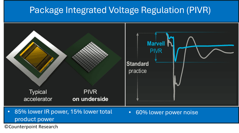
Another interesting example of custom silicon is Marvell’s on-package integrated voltage regulation chip (PIVR). Delivering power to an accelerator chip along its PCB typically results in substantial power loss and inefficiencies. Instead of being a separate chip located several inches away from the processor chip, the PIVR chip is integrated under the processor chip itself (Figure 2, left). This significantly reduces transmission losses while allowing more power to be delivered to the processor. With package-regulated voltage regulation, Marvell’s PIVR chip reduces power loss by 85% while achieving a 15% reduction in total product power. In addition, the PIVR chip enables a 60% reduction in power noise (Figure 2, right). Denser power delivery results in more compute per rack, which in turn results in increased ROI for data center operators.
Marvell Socket Wins
Marvell currently has 18 custom silicon socket wins (5 custom XPUs and 12 custom attach). Each custom XPU is a multi-billion dollar opportunity with a typical life cycle of 18-24 months while each XPU attach represents a multi-million dollar opportunity over 2-4 years. The company is also evaluating around 50+ other opportunities across 10 potential customers. Around one-third of these opportunities are for XPUs while the remainder are XPU attach opportunities. Marvell is targeting a 20% share of the AI data center silicon market, representing a value of more than $18 billion by 2028.
Ecosystem Opportunities
In addition to custom silicon component announcements, Marvell recently made two strategic ecosystem announcements. Firstly, it announced that it is joining Nvidia’s NVLink Fusion initiative. Shortly afterwards, it announced that it had developed a customizable compute platform based on the Ultra Accelerator Link (UALink) standard:
Nvidia’s NVLink Fusion – partly opens Nvidia’s NVLink compute fabric and rack architecture to third-party silicon, allowing partners to integrate custom XPUs seamlessly into Nvidia-based rack infrastructure. This provides a fast route to scale AI factories to millions of accelerators using custom XPUs. Alternatively, partners can plug their own custom CPUs into Nvidia’s GPU rack systems.
UALink - Marvell has developed a customizable UALink scale-up solution, with 224G SerDes and UALink physical layer IP, together with a range of advanced packaging options optimized for specific hardware configurations and performance/power targets. UALink competes with NVLink on performance but brings open-standards and multi-vendor flexibility to hyperscale AI infrastructure. It enables customers to deliver scale-up interconnects for up to 1,024 coherently-connected accelerators in a single pod.
Analyst Viewpoint
The trend toward customization in AI data center infrastructure is clear and accelerating, particularly amongst the biggest players. Indeed, customization is becoming strategically essential for any company deploying AI at scale as it enables optimum performance/Watt while enabling greater control of innovation, security and ecosystem supply chains. Custom silicon is no longer confined to compute but includes virtually all components, including interconnects, power components, switches, storage and security, enabling hyperscalers and other AI infrastructure players to build vertically optimized, high-performance, energy-efficient AI factories.
However, developing custom AI silicon requires deep expertise across multiple domains and vendors must be able to satisfy a range of technical, strategic and operational requirements. In this new era of cloud optimized silicon, it is therefore vital to work with a full-service partner. Marvell’s AI strategy is based on leveraging core IP in critical technologies - such as SerDes, Die-to-Die (D2D) interconnects and advanced packaging - to develop custom products and solutions, in collaboration with major players in the data center market. In fact, Marvell has become a one-stop shop for a range of custom silicon products and services. This means that customers do not need to aggregate IP from third party companies, hire a design house to complement their own in-house teams or find vendors to manage supply chains.
Counterpoint Research believes that Marvell’s recent NVLink and UALink announcements are strategically significant and will enhance the company’s standing as a key “go-to” silicon provider for accelerated custom AI infrastructure. By integrating NVLink Fusion into its custom cloud silicon, Marvell’s becomes a “drop-in ready” supplier for cloud providers already using Nvidia’s rack systems. This puts the company in a strong position to secure new design and integration wins, while its customizable UALink IP solution positions it as a major enabler and integrator of next-generation AI infrastructure using open standards.
By supporting both initiatives, Marvell cleverly increases its data center custom silicon TAM, enabling it to target Nvidia customers interested in custom silicon solutions as well as customers looking for alternative, high-performance AI fabrics based on open standards.


