- NVIDIA’s optics strategy is based on vertical integration and an aggressive first-to-market strategy supported by a number of key strategic investments in the optical supply chain.
- NVIDIA is adopting a unified photonics strategy with the same optical hardware used across Quantum, Spectrum, and NVLink switches and other components to minimize manufacturing costs.
- Although NVIDIA’s strategy is based on vertical integration, it also backs open standards such as the OCI MSA, where it makes sense.
At GTC 2025, NVIDIA unveiled its first Co-Packaged Optics (CPO)-based switches, with two networking products: the Quantum-X800 InfiniBand switch and the Spectrum-X800 switch, an Ethernet version of the same switch. At GTC 2026, NVIDIA outlined a more detailed and expansive roadmap of how it will transition to optical networking.
Blackwell Platform
Although GB200 NVL72 systems mostly ship with standard pluggable optics (ConnectX-7 /400G or 800G), they can be configured with CPO-based switches for massive clusters.
However, for Blackwell Ultra-based GB300 NVL72 racks, the Quantum-X800 and Spectrum-X800 CPO-based switches are the preferred high-efficiency choice. Although traditional pluggable OSFP[1] modules can still be used, the CPO version is marketed as the "performance" standard for the GB300 NVL72 racks to handle the higher power and thermal demands of the Blackwell Ultra chips. Moving optical components closer to the switch ASIC significantly reduces power consumption and signal degradation compared to copper or fiber. A single QuantumX-800 or SpectrumX-800 switch can support up to 144 ports of 800 Gb/s, allowing for flatter networks with fewer switches and lower hops.
Vera Rubin Platform
In contrast to the Blackwell platform, the Vera Rubin platform will use Linear Pluggable Optics (LPO) at the NIC end instead of pluggable transceivers. Traditional pluggable transceivers use DSPs to maintain signal integrity between the NIC and the scale-out switch. However, as scale-out networks transition to 1.6 Tb/s, this results in massive power consumption and heat. With an LPO-based design, the DSPs in the NIC and the switch are used to maintain signal integrity.
The biggest difference between the Blackwell and Vera Rubin platforms will be in the scale-up domain. Within the rack, the Vera Rubin platform still retains the all-copper design of previous NVIDIA rackscale systems. However, to cater for scale-up across multiple racks, NVIDIA is introducing a special CPO-based NVLink switch to create NVL576 (8 rack) pods.
NVLink Switch
The NVLink 6 switch used in the Vera Rubin platform is primarily an all-electrical switch chip, but its deployment in a rack depends on the specific hardware configurations of the racks. The switch comes in two varieties: a standard NVLink 6 switch and an NVLink 6 switch with CPO:
- Standard NVLink 6 Switch – in the standard Vera Rubin NVL72 rack, the NVLink 6 switch is all-electrical. It uses a massive copper midplane to connect the 72 GPUs in a single rack. The switch’s ports plug directly into the rack's copper spine.
- NVLink 6 Switch with CPO – for NVL576-sized pods, the NVLink switch adopts CPO. This is a specialized version of the NVLink 6 switch tray with integrated CPO, which uses micro-ring modulators to convert the electrical NVLink signals into light pulses and remote laser modules to send the NVLink signals over fiber to adjacent racks. However, the core of the switch is still electrical and processes data packets in the electrical domain.
Standard networking uses OSFP-based connectors. However, the NVLink 6 scale-up switch ports in the Oberon (NVL576) and Kyber (NVL1152) racks use OSFP-XD connectors. XD or "Xtra Density" doubles the number of electrical lanes in the same physical plug size. This allows a single port to handle the 1.6 Tb/s to 3.2 Tb/s bandwidth required to keep NVLink's "shared memory" performance across racks. Although it looks like a standard high-speed plug, the internal pin density is twice as high. Unlike traditional networking, where the transceiver contains a laser and a DSP chip, the scale-up NVLink cables are linear and consist of passive optical fiber.
A high-density fiber ribbon (MPO/MTP[2]) then connects directly into the OSFP-XD cage. By using a passive pluggable fiber instead of an active transceiver, NVIDIA eliminates the main cause of failure in data centers, i.e. overheating transceivers while reducing the latency to a minimum.
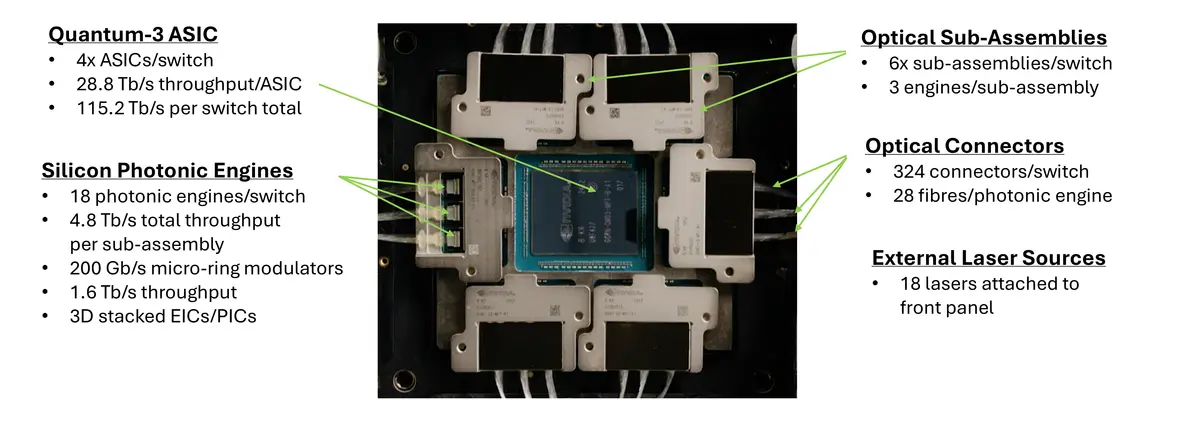
The graphic below shows the Quantum-3 ASIC together with detachable optical sub-assemblies used in NVIDIA’s Quantum-X800 Q3450-LD photonics switch.
Quantum-3 ASIC Used in NVIDIA’s Quantum-X800 Q3450-LD Photonics Switch
Feynman Platform
At GTC 2026, NVIDIA provided the first deep technical dive into the Feynman architecture due to be launched in 2028. Following the Blackwell and Rubin generations, Feynman is designed to be the backbone of "Gigawatt-scale" AI factories. The architecture shifts from simply connecting GPUs to a "system-of-systems" approach, utilizing advanced 3D stacking and optical interconnects to overcome the physical limits of copper.
Optical NVLink for Scale-up
In the Feynman platform, scale-up transitions from copper-based backplanes to native CPO. Feynman GPUs are designed to integrate silicon photonics directly onto the GPU package. NVIDIA is working on developing standalone I/O optical chips as well as integrated chips where the laser is integrated into the I/O chip. However, initial designs almost certainly will use remote rather than integrated lasers for reliability and serviceability reasons.
Optical Compute Interface (OCI)
NVIDIA is also expected to use the Optical Compute Interconnect (OCI) standard to attach CPO modules to its GPUs. Launched at OFC26 last month, the OCI Multi-Source Agreement (MSA) is one of several optical interconnect MSAs launched recently. NVIDIA has positioned itself as a founding member of the OCI MSA to ensure that all the optical components – lasers, fibers and silicon photonic connectors – become part of a standardized multi-vendor ecosystem.
OCI defines the physical and electrical layers, which include the electrical SerDes interfaces, packaging and pinout and the use of Wavelength Division Multiplexing (WDM) – specifically the 4-wavelength (Gen 1) and 8-wavelength (Gen-2) configurations. However, the logical layer will still use NVIDIA’s proprietary NVLink standard.
NVLink 8 Switch
The roadmap with respect to the precise technology used in the NVLink switch is still currently unclear. Based on NVIDIA’s latest roadmap, it is possible that NVLink 8 will remain a CPO-based electrical packet switch as with NVLink 6/7. However, it is not inconceivable that NVIDIA will transition to Optical Circuit Switching (OCS) or a similar technology. NVIDIA recently signed a $2-billion agreement with Lumentum, a company with extensive expertise in OCS technology and a supplier of the MEMS-based mirror system used in Google’s Palomar scale-up fabric. Another possibility is that NVIDIA may adopt a hybrid strategy, i.e. use electrical packet switching within switch trays but move to OCS for data transfers between racks.
3.2T Scale-out Networking
Although the initial Feynman racks will use 1.6 Tb/s switches, later versions will use 3.2 Tb/s networking with next-generation switches, providing a total of 204.8 Tb/s bandwidth. As with Vera Rubin, the switches will be optimized for CPO, reducing the power-hungry "electrical-to-optical" conversion occurring in pluggable transceivers. The GPUs in Feynman are connected to a ConnectX-10 NIC, which supports 1.6 Tb/s per port ensuring the network can keep pace with the 3D-stacked compute engines. Finally, the BlueField-5 DPU will act as the "Data Center OS" for Feynman, offloading security, storage (via the CMX platform) and KV-cache management from the GPUs.
Analyst Take
NVIDIA’s optics strategy is based on vertical integration and an aggressive first-to-market strategy supported by a number of strategic investments in the optical supply chain. While competitors focus on being optics suppliers to everyone, NVIDIA is building an exclusive, end-to-end optical ecosystem designed specifically for its own AI Factories. However, the transition to optics will be a gradual process starting with CPO on scale-out switches on the Blackwell Ultra racks. Then CPO-based NVLink switches will be introduced on the Vera Rubin platform connecting multiple racks in 1,152 GPU-sized scale-up networks. CPO-native GPUs will only be introduced on the Feynman platform, leading eventually to an estimated 2,304 GPU-sized pods, based on an all-optical interconnect network. NVIDIA is also adopting a unified photonics strategy. Regardless of whether it a Quantum, Spectrum or an NVLink scale-up switch, the same optical hardware will be used across all product lines to minimise manufacturing costs.
NVIDIA thus controls the entire stack – from the GPUs and the NVLink switch to the software and the optical engines using its own silicon photonics technology. However, it is also backing open-standards, such as the OCI MSA – where it makes sense. In so doing, NVIDIA avoids being locked into a single supplier for optical components. It can thus use its own optical engines, lasers and other components, or buy OCI-compliant components from third parties if there is a supply shortage.
Note: An expanded version of this blog will be published as a 6-page report, available on Counterpoint Research’s website.
[1] Octal Small Form Factor Pluggable
[2] Multi-fiber Push-on/Multi-fiber Termination Push-on


