- One real product announcement: the TSMC ADK, an AI Design Kit that replaces the human-facing PDK with agents trained on TSMC's own design history. The rest of the event was about roadmap and partner certification.
- All three EDA houses certified A14 at the event, about two years ahead of production. Tool readiness is on track. What an agent does inside a certified flow becomes the key factor.
- TSMC has put DRAM-on-logic on its 2029 roadmap at around 3× HBM5E bandwidth under 1 pJ/bit. Our d-Matrix report in the series reached the same conclusion from the other direction.
- On optics, TSMC and GlobalFoundries are solving different problems. COUPE pulls the optical engine onto the TSMC package; GF's SCALE sells a merchant module to anyone. Both are built to the OCI spec, so the difference is where the engine sits. TSMC wins inside its own package, GF has the larger market.
- Some numbers did not agree across sessions: HBM stacks per package in 2028 came out as 16 in one session against 20 on TSMC's own roadmap slide. This is contradicting the current cutdown of HBM stacks we are seeing for various reasons.
- The strategy is bundling: each layer is replaceable on its own, the stack is not. Our foundry tracker has TSMC at 73% of pure-play revenue, and the ADK looks like how it defends that into the angstrom era.
Decoding TSMC's OIP announcements
TSMC held its 2026 North America OIP Ecosystem Forum on 23 September at the Santa Clara Convention Center, under the theme “Expanding AI with Leadership Ecosystem”. It is the design-side companion to April's silicon-side symposium.
The day ran as a TSMC welcome, a Broadcom ASIC keynote, a TSMC R&D keynote, a packaging block and then three parallel tracks. Around thirty talks on site, another thirty-five online for six months, and fifty to a hundred partners on the floor, including a new Emerging Technologies Alley for startups. TSMC's booth had a 9.5×-reticle CoWoS vehicle on display, which is the 2027 configuration; the largest CoWoS in production today is 5.5×. Cameras were restricted in the keynote hall, so the figures here come from our own notes.
OIP is the customer-facing side of the foundry rather than the technology-facing one. It now runs to about ninety members across six alliances. imec's IC-Link joined the Cloud Alliance with a managed environment that can run mixed Synopsys, Cadence and Siemens flows against TSMC PDKs.
The TSMC AI Design Kit was the highlight announcement with setting an example of how a foundry has started selling the design method itself.
The ADK is the key announcement
TSMC is positioning the move from human-centric PDK to the ADK. Agents learn from the foundry's own technology layers such as cell selection, pin escapes and routing strategy, and they run workflows rather than waiting for an engineer to drive them. Design centres and EDA partners are already feeding TSMC-specific data in. I think agents at this level will cut design time and accelerate design cycles, but who owns the data behind them, how the intelligence moves through the workflow, whose process intellectual property is being applied and who charges for it are all still unclear.
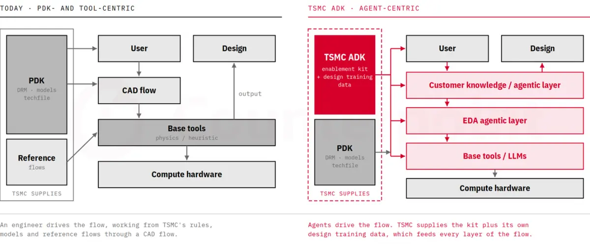
Figure 1 Source: Counterpoint Research, TSMC OIP 2026
Read the full report: $Trillion Bottleneck: Memory Wall :: TSMC's AI Design Kit, Packaging as a Product and 3D DRAM in 2029
Similar blogs from the series:
The $Trillion Bottleneck: Memory Wall :: Intel Bets EMIB, ZAM and XBM Against TSMC’s CoWoS
The $Trillion Bottleneck: Memory Wall :: Inside Qualcomm's High Bandwidth Compute (HBC) Bet
The $Trillion Bottleneck: Memory Wall :: NVIDIA's NVHBM and the Fight for the Base Die


